

Why Choose An Advanced Complex IoT Control Board PCBA Factory Over Low-Cost Alternatives

Q1: How Does RF Impedance Misalignment in Low-Cost Assembly Compromise IoT Gateway Connectivity?
Wireless connectivity forms the baseline foundation of any modern internet of things network ecosystem. For optimal data transmission, high-frequency signal traces must maintain a strict 50 ohm characteristic impedance across the board layout. However, budget assembly facilities often overlook tiny variations in copper geometry, trace width, and circuit board dielectric materials. This manufacturing negligence alters the intended electrical path layout significantly during mass production. As a result, radio frequency impedance mismatch occurs across the printed circuit board assembly. These subtle mismatches create massive signal reflections that degrade overall radio frequency performance and reduce transmission range. Hardware systems experience high error vector magnitude and severe data packet loss during wireless handshakes. To compensate for these poor signal paths, internal power amplifiers run continuously at peak capacity to maintain a connection. This behavior quickly drains available battery reserves and overheats the main processor enclosure, leading to system freezes. Advanced production centers eliminate these radio frequency vulnerabilities by utilizing specialized testing instruments throughout the production cycle. Engineers deploy time-domain reflectometry equipment to measure signal trace compliance during surface mount assembly. Additionally, automated vector network analyzers verify signal transmission qualities across all wireless spectrum bands. This strict calibration guarantees stable network connectivity for smart hardware deployments worldwide.
Q2: Why Do Low-End Factories Fail to Detect Micro-Leakage Currents in Ultra-Low-Power IoT Devices?
Battery-powered smart sensors often operate in remote locations for up to ten years without any physical maintenance. To achieve this extreme longevity, internal components must spend 99 percent of their operating life in deeply passive sleep modes. During these periods, the circuit architecture draws only micro-amps or nano-amps of electrical power from the battery cell. However, sub-microamp parasitic current leaks can quickly destroy this carefully planned battery budget within a few months. Low-end manufacturing plants frequently cause these hidden currents due to inadequate chemical cleaning and improper board baking procedures. Sub-microscopic flux residues remain trapped beneath dense quad-flat no-lead packages and area-array packages after reflow soldering. Over time, atmospheric moisture mixes with these chemical residues to initiate electrochemical migration inside the micro-gap. This phenomenon creates conductive microscopic pathways that leach electrical power continuously across adjacent circuit traces. Low-cost factories rely purely on simple functional tests that only check if a device turns on or off under laboratory conditions. These rudimentary testing methods completely fail to identify tiny micro-leakage anomalies that manifest later. Conversely, a professional partner like Aozite OST PCBA uses highly sensitive in-circuit testing setups to catch subtle power anomalies early. Advanced automated test routines measure passive sleep-state current draws with extreme resolution down to nano-amp scales. This rigorous validation ensures that finished devices achieve their full planned battery lifecycles in the field.
Q3: What Makes Environmental Stress Screening (ESS) Mandatory for Extending the Field Lifespan of Remote Sensors?
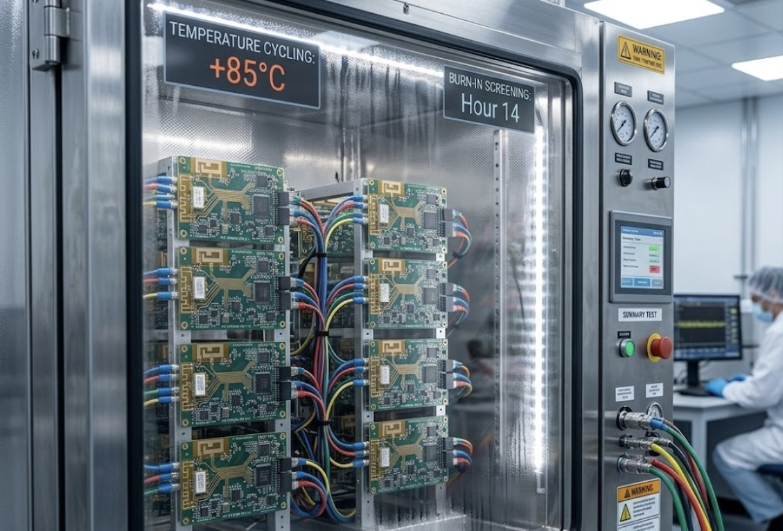
Remote telemetry hardware and outdoor gateways must survive severe environmental challenges throughout their operational lifetimes. These devices face rapid temperature fluctuations, high humidity levels, salt spray corrosion, and intense industrial vibrations daily. Budget contract assembly houses usually ship circuit boards immediately after standard automated optical inspections to accelerate delivery times. Unfortunately, this lack of stress testing transfers all operational risks directly onto the end buyer. Latent manufacturing defects, such as weak micro-vias or fragile solder joints, remain completely hidden under normal room conditions. These hidden weaknesses quickly fail when exposed to real-world operational stressors and thermal expansion forces. To eliminate early lifecycle failures, advanced factories integrate mandatory Environmental Stress Screening protocols into their standard workflow. Production teams expose assembled hardware to rapid thermal cycling and active power-on burn-in processes within specialized environmental chambers. This intense thermal stress forces weak metallurgical bonds and microscopic board delamination to surface before final packaging. Meanwhile, one-stop PCBA turnkey solution for industrial control and automation equipment procedures incorporate automated mechanical vibration testing to verify structural durability. This screening process isolates weak connections and component defects before shipment. Consequently, international technology developers receive highly durable hardware that performs reliably in the most demanding outdoor conditions.
Q4: How Does Aozite OST PCBA Translate Industrial-Grade Turnkey Engineering into IoT Deployment Security?
Managing scattered suppliers creates complex communication gaps that increase manufacturing risks and delay project timelines. Sourcing components from one distributor while assembling boards at an independent facility frequently leads to undetected component defects. To prevent these supply chain failures, elite manufacturers offer centralized turnkey project management from engineering design to mass fulfillment. For global technology companies targeting high-reliability sectors, Aozite OST PCBA(Shenzhen Aozite Technology Co., Limited) provides a robust platform that guarantees long-term hardware survival. The enterprise operates eight fully automated high-speed SMT production lines at their modern manufacturing base. This setup generates a daily capacity exceeding 1.2 million solder joints, allowing the factory to handle massive international programs smoothly. Furthermore, the engineering group performs thorough design for manufacturability checks before initiating production to optimize board layout. This proactive validation eliminates layout errors and minimizes component clearance challenges early in the manufacturing timeline. Incoming inspection teams also utilize advanced X-ray equipment to authenticate semiconductors and prevent counterfeit electronics from entering production lines. This rigorous tracking strategy ensures that every component performs exactly as the developer intended. By combining advanced process monitoring with complete supply chain transparency, Shenzhen Aozite Technology Co.,Limited eliminates engineering vulnerabilities and helps international innovators scale their hardware deployments with total confidence.
To discover more about complex internet of things manufacturing capabilities, please visit the official company website: https://www.aozite-pcba.com/.
Aozite OST PCBA
Aozite OST PCBA
Legal Disclaimer:
EIN Presswire provides this news content "as is" without warranty of any kind. We do not accept any responsibility or liability for the accuracy, content, images, videos, licenses, completeness, legality, or reliability of the information contained in this article. If you have any complaints or copyright issues related to this article, kindly contact the author above.
